For the last decade, numerous chemical synthesis methods have been developed for the fabrication of functional nanomaterials. However, the integration of bottom-up synthesized nanomaterials in devices has been a great challenge with poor controllability, reproducibility, and reliability. Our group has put great efforts to develop various hybrid nanomanufacturing processes by combining the advantages of top-down and bottom-up nanofabrication methods.
2-1. Guided self-assembly of functional nanomaterials:
2-1-1.
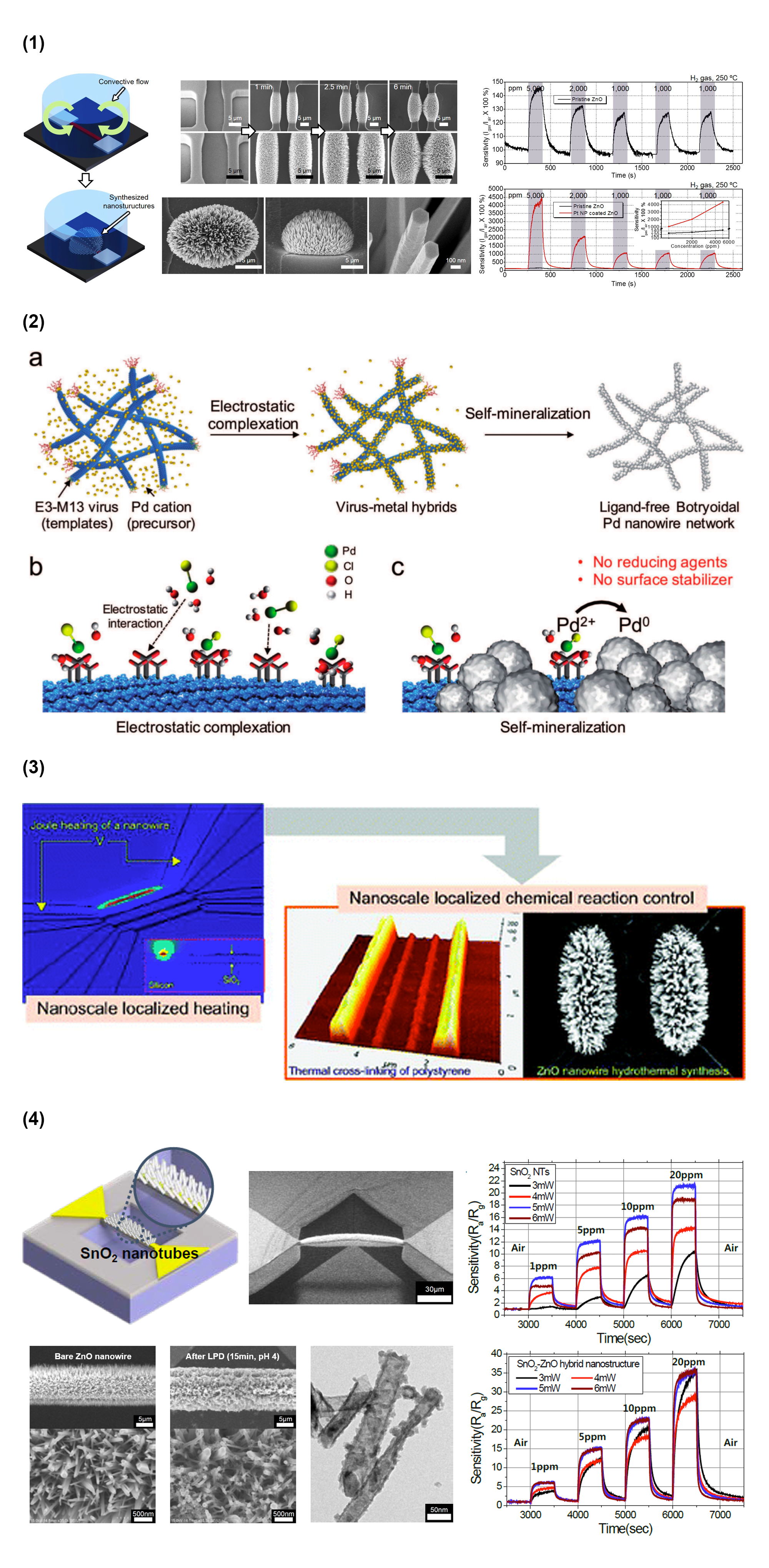
- Direct and large-scale micro/nano-patterning of functional nanomaterials:We developed direct nanoimprinting lithography where liquid solution of functional nanomaterials can be used as an ink for the nanoimprinting-based direct nanopatterning process [34-37]. Also, transfer printing process was employed for the large area direct formation of micropatterns of nanomaterials [38]. Furthermore, we have developed a low-cost, large scale nanofabrication of silicon nanomesh via nanosphere lithography of polystyrene beads and plasma etching process [15]. These direct micro/nano-patterning methods can realize facile fabrication of electronic devices such as sensors and field effect transistors.
2-1-2.
- Templated assembly of nanomaterials and synthesis of functional nanostructures: Metal nanoparticles such as platinum (Pt), palladium (Pd) or silver (Ag) can be used as catalysts for functional devices such as sensors, fuel cells, batteries, etc. We have developed liquid-phase method for the templated synthesis and assembly of metal nanoparticles along the nanowires, instead of vacuum deposition (eg. sputtering or evaporation) [39-41]. By controlling the synthesis parameters (concentration, temperature, time, etc.), we can either form metal-metal oxide hybrid nanostructures or metal nanotubes. Furthermore, multi-metallic nanotubes can be easily fabricated by mixing multiple metal precursors [42]. Also, we developed a facile liquid phase synthesis method of metal nanofibers using virus as a one dimensional template [43].
[34] S-H. Ko, I. Park, H. Pan, C.P. Grigoropoulos, A.P. Pisano, C. K. Luscombe, and J. M. J. Frechet, “Direct Nanoimprinting of Metal Nanoparticles for Nanoscale Electronics Fabrication”, Nano Letters 7,1869-1877, Jun 2007
[35] I. Park, S-H. Ko, H.Pan, E-S. Lee, J-H. Jeong, A.P. Pisano, C.P. Grigoropoulos, and J.M.J. Frechet, “Nanoscale Patterning and electronics on flexible substrate by direct nanoimprinting of metallic nanoparticles”, Advanced Materials 20, 489-496, Jan 2008
[36] S-H. Ko, I. Park, H. Pan, N. Misra, M.S. Rogers, A.P. Pisano, and C. P. Grigoropoulos, “ZnO nanowire network transistor fabrication on a polymer substrate by low-temperature, all-inorganic nanoparticles solution process”, Applied Physics Letters 92, 154102, Apr 2008
[37] E-U. Kim, K-J Baeg, D-Y Kim, Y-Y Noh, D-Y. Kim, T. Lee, I. Park*, and G-Y. Jung*, “Templated assembly of metal nanoparticles in nanoimprinted patters for metal nanowire fabrication”, Nanotechnology 20, 355302, Aug 2009
[38] S. Kim, W. S. Lee, J. Lee, and I. Park, “Direct micro/nano metal patterning based on two-step transfer printing of ionic metal nano-ink”, Nanotechnology 23, 285301, Jun 2012
[39] M. Lim, Y. Lee, S-W. Han, and I. Park, “Novel fabrication method of diverse one-dimensional Pt/ZnO hybrid nanostructures and its sensor application”, Nanotechnology 22, 035601, Jan 2011
[40] Y. Lee, M. Lim, I. Park, and S-W. Han, “Facile Synthesis of Noble Metal Nanotubes by Using ZnO Nanowires as Sacrificial Scaffolds and Their Electrocatalytic Properties”, Chemical Communications 47, 6299-6301, Apr 2011
[41] M. Lim, D. Kim, C-O. Park, Y. Lee, S-W. Han, Z. Li, R.S. Williams, and I. Park, “A new route towards ultra-sensitive, flexible chemical sensors: metal nanotubes by wet-chemical synthesis along sacrificial nanowire templates”, ACS Nano 6, 598-608, Dec 2011
[42] B-S. Choi, Y. W. Lee, S. W. Kang, J. W. Hong, J. Kim, I. Park, and S. W. Han, “Multi-Metallic Alloy Nanotubes with Nanoporous Framework”, ACS Nano 6, 5659-5667, May 2012 (* co-corresponding authors)
[43] I. Kim, K. Kang, M.H. Oh, M.Y. Yang, I. Park, and Y.S. Nam, “Virus-templated Self-mineralization of Ligand-free Colloidal Palladium Nanostructures for High Surface Activity and Stability”, Advanced Functional Materials 27,1703262, Nov 2017
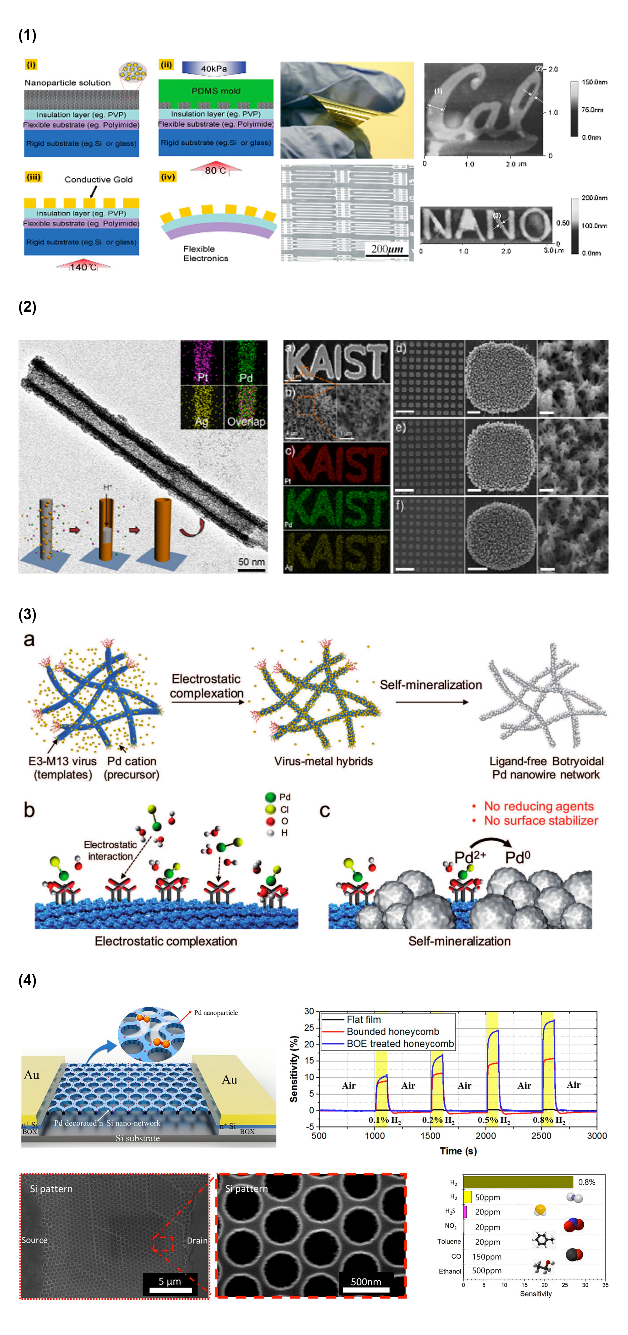
Figure 4. Guided self-assembly of functional nanomaterials: (1) direct nanoimprinting of metal nanoparticles for flexible nanoelectronics fabrication (I. Park, et al., Advanced Materials 2008), (2) Templated synthesis of multimetallic nanotubes (I. Park, S-W. Han, et al., ACS Nano 2012), (3) liquid-phase synthesis of metallic nanofiber using virus template (I. Park, Y-S. Nam, et al., Advanced Functional Materials 2017), and (4) large scale nanomesh fabrication using nanosphere lithography of polymer beads (I. Park, et al., Small 2018)